Meet the 3410 RAM Component
CS3410 Component Guide
tl;dr There is no tl;dr. You just have to read the whole thing ¯\_(ツ)_/¯
Inputs and Outputs
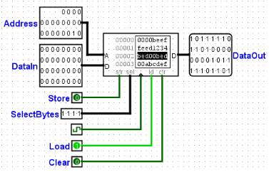
A is the word-address. Each line in the RAM component is a word (four bytes) in memory, and has a unique address. As in the example figure to the right, A = 0x00002 refers to slot 00002 in the RAM component, which contains a full word. However, for a given address in RAM, if you want to retrieve a specific byte or halfword in the address, you need to use the selector bits (described below). By default, the component's address width is 20 bits (which means that, by default, it can store 2^20 words = 4 * 2^20 bytes = 4MB).D contains the data to be stored in RAM. Depending on how sel is set, only certain bytes within D will be written.
str is the store bit. You can think of it as Write Enable. When str = 1, RAM will write the value on D to address A according to the sel bits.
sel is for the selector bits. As mentioned above, bits 0..7 of D correspond to sel = 0001, bits 8..15 correspond to sel = 0010, bits 16..23 to 0100, and bits 24..31 to 1000. sel accepts other combinations like 1100 (to grab the upper halfword), 1111 (to grab the full word), or even something wacky like 1010.
ld is the load bit. Data Out D always sets floating values (X's) along the wire unless the appropriate selector bits are set and ld = 1.
clr clears all of RAM whenever it is 1.

Using the Byte Selector
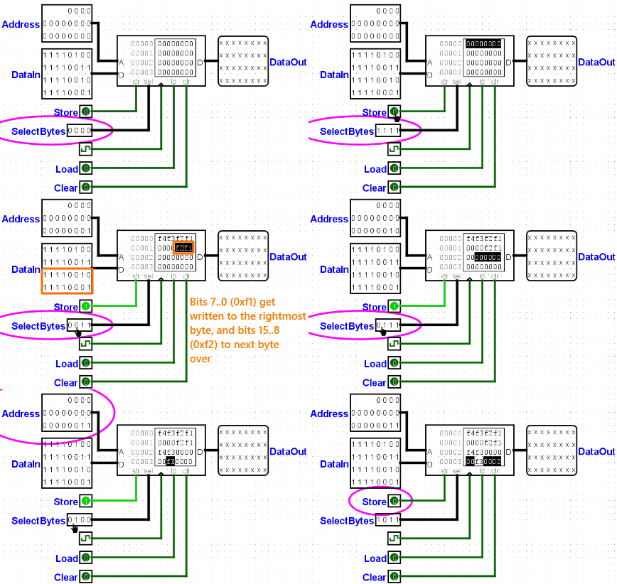
As previously mentioned, address A gets us to the word in memory. However, we need to use sel to determine which bytes in the word we want to write to or read from. The Byte selector is 4 bits, and you can think of each bit as a read/write enable for each of the four bytes in the word.Specifically, bit 0 of sel enables the first byte from the right in the RAM component. When writing to RAM, bits 0 to 7 of DataIn are written to this byte, and when reading from RAM, the byte's value gets read out to bits 0 to 7 of DataOut. Bit 1 of sel enables the second byte from the right, and corresponds with bits 8 to 15 of DataIn and DataOut. Bit 2 enables the third byte from the right and corresponds with bits 16 to 23, and bit 3 enables the fourth byte, and corresponds with bits 24 to 31.
Storing
Writing into the RAM component requires that the str bit is set to 1.
When you want to write a byte to a location in RAM, pay attention that you place the byte-values in DataIn correctly with selector bits. In the example above, if you wanted to write 0xf1 to left-most byte, you would need to put 0xf1 in bits 24..31 in DataIn and set sel = 1000.
Loading
Reading from the RAM component requires that the ld bit is set to 1.