Group Project 2 - Fully Pipelined MIPS
This is cumulative. Both Table A and Table B instructions are required.
CS3410 Spring 2014
Work-in-progress Circuit Due: 11:59pm, Monday, March 17, 2014
Final Design Due: 11:59pm, Thursday, March 27, 2014
Late Policy: Start early, don't be late.
You must work in the same group for this project as for the last.
Overview
In this project you will extend and complete the processor design you started in project 1. Your basic execution loop from the previous assignment should contain most of the major components, with the exception of RAM for the load/store instructions. For this project we will use a split-memory "Harvard" architecture design: The Program ROM will store a read-only copy of the instructions, and a separate RAM will be used to store data for the program's execution. You will now implement all the other instructions mentioned in the last project project, including load/stores, jumps and branches.
You should reuse most or all of your work from project 1. This means updating the circuit circuit to handle the new instructions, revising the documentation to discuss any changes or addition to the datapath and control logic, and expanding your test program. This includes, of course, fixing anything that was broken or incomplete from the first project (ask the staff for help if needed — we will not be posting a solution, but neither do we want to penalize you twice for mistakes in project 1).
Important:Consult the MIPS Handbook and make sure that all aspects of each of the instructions is implemented exactly as specified in the handbook, except where noted here.
Academic Integrity As one of the most widely studied architectures, MIPS has a wealth of information available on the web and in textbooks. You may consult any of the MIPS architecture documentation available to you in order to learn about the instruction set, what each instruction does, etc. But we expect your design to be entirely your own. If you are unsure if it is okay to borrow from some other source, just ask the TAs, and give credit in your final writeup. If you are unsure about asking the TAs, then it is probably not okay. Plagiarism in any form will not be tolerated.
What to Implement
Implement all of the instructions in Table B. You should have already decoded all these instructions in project 1. You may have to add additional decoding logic for any new control signals you introduce, as for the memory stage and for the PC update.
| Table B | |
| Jumps (with one delay slot) | J, JR, JAL, JALR |
| Branches (with one delay slot) | BEQ, BNE, BLEZ, BGTZ, BLTZ, BGEZ |
| Memory Load/Store (little endian, with pipeline stall if needed) | LW, LB, LBU, SW, SB |
Our testing programs will include a mixture of all the instructions from projects 1 and 2, so you must ensure that the instructions from project 1 are correctly implemented as well.
Deviation from the MIPS standard: You can ignore any MIPS instruction or feature not mentioned in this document, such as traps, exceptions, and system calls. You can also assume that your processor will never encounter anything but legal instructions from Tables A and B.
Refer to the MIPS manual, Volume 2, linked on the course web site for a full specification of what each of these operations does. Except where noted in here, the MIPS manual is the authoritative specification for this project: information you find elsewhere (e.g. Wikipedia or the book) doesn't count if it contradicts the MIPS manual.
Delay slot. You must properly implement the branch/jump delay slot, so that the instruction immediately following a branch or jump is always executed, and any relative addresses or significant bits for the PC update are based on the that address and not the address of the jump instruction itself.
Memory load hazard. Memory operations should not have delay slot, but instead use stalling to avoid hazards. That is, you should introduce a bubble in the pipeline after a memory operation, but only if a hazard is detected.
RAM. The cs3410.jar Logisim library on the course web site includes a MIPS
RAM component for your memory stage (see the description below). Logisim does not support RAM components large
enough to cover a full 32-bit (4GB) address space. The largest RAM component contains 64MB of data using 24-bit-wide
word-addresses. Our tests will rely on memory addresses in the lowest 1MB of the address space, so your your processor
should contain at least 1MB of RAM placed at the lowest addresses. That is, reads and writes to byte-addresses
in the range 0x00000000 to 0x000fffff should work as expected.
Important: Writes to addresses that not backed by any RAM should
have no effect, and the address space should not "wrap around" after 1MB.
For the adventurous. Instead of having a single RAM component backing the low part of the address space, you can add multiple RAM components to cover various convenient pieces of the address space. For instance, to support the conventional MIPS program layout, put a second RAM to cover a few MB of address space near addresses 0x10000000 for program data, and a third RAM to cover addresses just under 0x80000000 for the stack. Or you can redirect reads and writes at certain addresses to some of Logisim's input/output devices. It is actually fairly trivial to make writes at addresses just above 0x80000000 write coordinate and color pixel data to an LCD screen component or ASCII characters to a TTY component. Similarly you can make reads at some designated unused address read from a Logisim Keyboard, Joystick, or other input component. Bonus points if you can code pong to go with an LCD.
Processor Components
As in project 1, build your MIPS processor as a single Logisim circuit file. Continue to use the same cs3410.jar library that we provided. Do not use Logisim's Project > Load Library > Logisim Library command to import circuits from other Logisim files.
Your top-level circuit must be named either "MIPS" or "MIPS32" (case-sensitive).
Your processor should have only one instance of each of these components: Register File, MIPS Program ROM, and ALU.
The restriction on incrementers has been relaxed since project 1: You may now use more than one incrementer, although incrementing PC by 4 should still be done with one incrementer rather than four.
You can additionally use any of the components that come with Logisim, such as a Register for the PC, multiplexers, and so on.
Testing
Write a test program in MIPS assembly that fully tests all of the features from both project 1 and project 2. As before, the program should be well commented, indicating what it is doing and what results should be expected when running the program, so that the course staff is convinced of the correctness of your processor.
We would also like you to test your program on a complex computation. A hailstone sequence is defined as follows: start at any positive integer n; if n is even, divide it by 2 to get n/2; else triple it and add one to get 3n+1; then repeat with the new number. You will implement the hailstone function, which counts how many steps it takes for the hailstone sequence to converge to 1 from a given starting point. For instance, hailstone(40) returns 8 because the sequence starting at 40 converges in 8 steps: 40, 20, 10, 5, 16, 8, 4, 2, 1. And hailstone(31) returns 106 due to its long and chaotic sequence: 31, 94, 47, 142, 71, 214, ..., 3077, 9232, 4616, 2308, 1154, 577, ..., 53, 160, 80, 40, 20, 10, 5, 16, 8, 4, 2, 1.
There are several ways to compute the hailstone function. You will implement all three of the methods below.
Recursive hailstone: Simple but inefficient. Logisim will be too slow to use this version except when the sequence converges quickly.
    int r_hailstone(int n) {
        if (n == 1) return 0;
        else if ((n % 2) == 0) return 1 + r_hailstone(n/2);
        else return 1 + r_hailstone(3*n+1);
    }
Iterative hailstone: An efficient approach for computing the answer for just a single sequence.
    int i_hailstone(int n) {
        int i = 0;
        while (n != 1) {
            i = i + 1;
            if ((n % 2) == 0)
                n = n/2;
            else
                n = 3*n+1;
        }
        return i;
    }
Memoization hailstone: For computing the answer for more than one sequence, it makes sense to remember previously computed answers since many sequences overlap. So if hailstone(40) has already been computed, then it is easy to compute hailstone(160) since its sequence is identical to the one for 40 after just 2 steps. This memoization version is essentially the same as the recursive version but takes two extra arguments: an array A of previously computed answers (should be initialized to all zeros), and the number of entries s in the array.
int m_hailstone(int n, int A[], int s) { if (n < s && A[n] != 0) return A[n]; /* computed this one before */ if (n == 1) return 0; else { int i; if ((n % 2) == 0) i = 1 + m_hailstone(n/2, A, s); else i = 1 + m_hailstone(3*n+1, A, s); if (n < s) A[n] = i; /* save this answer for reuse later */ return i; } }- Submit a work-in-progress version of your MIPS circuit on CMS
- Submit a README file stating what has and has not been implemented
- A single Logisim project file containing your processor and all needed subcomponents.
- A PDF file documenting your processor, including a processor block diagram and description of control logic.
- A text file containing your well-commented MIPS assembly test program.
- Three text files containing the three hailstone implementations in MIPS assembly.
Implement these three versions of the hailstone function using MIPS assembly code. They must all work on your processor in Logisim, though you will have be careful when testing to selecting starting values that converge in a reasonable time.
For the interested student: It is an open question whether all starting points eventually converge to 1 or not. Numbers that do converge are sometimes called wondrous numbers or hailstone numbers. The Collatz conjecture states that all positive integers are wondrous, but this isn't yet proven. For this project, you can assume all numbers converge — if you find one that doesn't you get an automatic A for the project. You can find links to more reading on the Wikipedia page for the Collatz conjecture.
Work-in-progress Circuit
Halfway through the project, you will submit a work-in-progress version of your circuit.
At the very least, you need to fix all the errors you had in PA1. We will provide feedback to your PA1 circuit. We expect the work-in-progress circuit to work perfectly on PA1 functionalities.
Your submitted work-in-progress circuit should be functional, NO red wire, NO undefined output. It is OK to miss some features, but it is not OK to submit a circuit that does not run PA1 test cases.
Documentation
Document your design in the same fashion as project 1. Be sure to revise your block diagram to show any new components, and to revise your descriptions of control and instruction decoding logic to account for any changes or additions.
What to Submit
Note the different due dates
By Monday, March 17, 2014
By Thursday, March 27, 2014
Help and Hints
MIPS calling conventions and program layout. The three versions of hailstone must be implemented as functions: they should take arguments and return results in registers (or on the stack), and use a call stack for recursive invocations. For this project, you are not required to follow MIPS calling convention precisely. However, it would be smart to at least roughly follow the MIPS register usage and calling conventions. Neither do you have to follow the conventional program layout precisely, since your processor likely does not have enough RAM to support the standard anyway.
Fibonacci and other MIPS code online. A favorite assignment is implementing recursive, iterative, or memoizing Fibonacci functions. You can find MIPS implementations of this and much more online. GCC and other tools can also generate MIPS code for you. Feel free to use any online sources (but not from your classmates, obviously) by borrowing or adapting code as you see fit, or by using any other tool that is convenient for you. For instance, you might borrow function entry and exit code from an online example of Fibonacci, but replace the body with code for hailstone. Or you might obtain some of your test code by modifying the MIPS output of some compiler. In all cases: you must provide attribution by citing your sources, either in your documentation or directly in your code. And, you are ultimately responsible for what you turn in, so you had best understand everything you submit.
cs3410 Component Library Guide
The cs3410 Component Library is available on the course web page.
Loading the cs3410 library From Project > Load Library > Jar Library... select the cs3410.jar file. You should now have a new folder in your sidebar containing the following components:
|
MIPS RAM. This component is identical to Logisim's regular 32-bit wide, word-addressed RAM component, except the single-bit sel input is replaced by a 4-bit input to selectively enable or disable access to individual bytes within a 32-bit word. For instance, if the memory contains the word 0xAABBCCDD at the current address, then sel=0011 will access only the least significant halfword (0xCCDD), and sel=1000 will access only the most significant byte (0xAA). This component does not have a defined endianness since it is word addressed. Byte addressed memory (either little-endian or big-endian) can be emulated: to access byte-address 4 (the fifth byte in memory) in little-endian mode, one would set a=1 (second word) and sel=0001 (least significant byte); to access byte-address 4 (the fifth byte in memory) in big-endian mode, one would set a=1 (second word) and sel=1000 (most significant byte). |  |
|||||||||||||||||||||||||||||||||||||||||||||
|
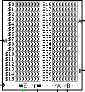
Register File. A 32-bit wide by 32-registers deep register file. Register $0 is hard-wired to zero at all times, and writes to $0 are ignored. Inputs rA and rB are used to select register values to output on the A and B outputs. When the clock is triggered, if WE is high, the data value at input W is stored in register rW. The register file can be configured to use rising clock edges as trigger (the default), falling edge, or to be level sensitive. |
 |
|||||||||||||||||||||||||||||||||||||||||||||
|
MIPS Program ROM. A 32-bit wide byte-addressed ROM, with built-in MIPS assembler. Use the attributes panel to load a MIPS assembly file into the ROM. The PC input specifies the address of the current instruction, and must be a multiple of 4. The output is the 32-bit machine code instruction at the PC address, or an error if the PC is invalid. Reading addresses outside the range of code supplied by the assembly file will cause the ROM to output zero, which happens to encode a no-op in MIPS. The assembly language is in the format described below. |
 |
|||||||||||||||||||||||||||||||||||||||||||||
|
MIPS ALU. Computes a result as follows:
|
 |
|||||||||||||||||||||||||||||||||||||||||||||
|
Incrementer. An adjustable-width incrementer. Takes its input A on the left and outputs A+1 on the right. |
|
|||||||||||||||||||||||||||||||||||||||||||||
|
LCD Video. If WE is high on the rising edge of CLK, writes a pixel on the LCD screen at the location given by the 7-bit unsigned X and Y coordinates. The pixel color is specified by 16-bit RGB input (in 5-5-5 format). The RST input resets the LCD screen. With some cleverness, you can redirect memory writes to this device to let your program draw on the LCD screen. Logisim also comes with some interesting input and output devices which can be used similarly. |
 |
MIPS (subset) Assembly Syntax
The MIPS Program ROM component has a built-in assembler that understands all of the instructions you will implement. The syntax is standard MIPS syntax. Labels are case sensitive, everything else ignores case. Anything following a pound ('#') is a comment. In project 1, you will only use a few of the instructions listed here.
The instruction syntax is the same as given in the MIPS standard (and different from the output of gcc and many other tools). Registers are written as $0, $1, ..., $31, and the destination register goes on the left, followed by source registers and immediate values on the right. Most integer arguments (immediates, shift amounts, jump targets) can be specified in hex (i.e. 0x12ab), in decimal (i.e. 1234 or -1234), a label, or the special constant PC. The assembler will replace PC with the address of the instruction itself. Most constants have some restrictions: jump destinations must have the same upper 4 bits as the PC+4, and must be a multiple of 4; branch destinations must be a multiple of 4 and fit in a signed 18 bit immediate; etc. As a special case, when a branch target is specified symbolically as a label, the assembler will automatically subtract the current PC value to obtain a signed offset.
By default, the first instruction will be placed at address 0, and subsequent instructions are placed at at addresses 4, 8, 12, etc.
Assembler directives. The Program ROM assembler understands two standard MIPS assembler directives, .text and .word, both of which take integer (hex or decimal) arguments. For example, .text 0x50000000 will direct the assembler place subsequent instructions starting at address 0x50000000. And .word 0x24030005 directs the assembler to use the value 0x24030005 as the next machine instruction, which happens to be the machine code for ADDIU $3, $0, 5.
Some examples of instructions are:
| Immediate Arithmetic | ADDIU $12, $0, PC |
| Register Arithmetic | ADDU $13, $0, $20 |
| Immediate Load | LUI $14, 0x123 |
| Shifts | SLL $13, $13, 2 SLLV $15, $14, $3 |
| Jumps | J 0x24 J my_label JR $5 JALR $31, $5 JALR $5 |
| Branches | BEQ $5, $6, -12 BEQ $5, $6, my_loop_top BLEZ $9, 16 BLEZ $9, my_loop_done |
| Memory Load/Store | LW $12, -4($30) SW $12, 0($30) |
MIPS (subset) Opcode Summary (from the MIPS Handbook)
Items in white are required for project 2. Make sure to implement all of them.
| opcode | bits 28..26 → | ||||||||
| ↓ bits 31..29 | 0 | 1 | 2 | 3 | 4 | 5 | 6 | 7 | |
| 000 | 001 | 010 | 011 | 100 | 101 | 110 | 111 | ||
| 0 | 000 | SPECIAL δ | REGIMM δ | J | JAL | BEQ | BNE | BLEZ | BGTZ |
| 1 | 001 | ADDI | ADDIU | SLTI | SLTIU | ANDI | ORI | XORI | LUI |
| 2 | 010 | COP0 δ | COP1 δ | COP2 θδ | COP3 θδ | BEQL φ | BNEL φ | BLEZL φ | BGTZL Φ |
| 3 | 011 | β | β | β | β | SPECIAL2 δ | JALX ε | ε | * |
| 4 | 100 | LB | LH | LWL | LW | LBU | LHU | LWR | β |
| 5 | 101 | SB | SH | SWL | SW | β | β | SWR | CACHE |
| 6 | 110 | LL | LWC1 | LWC2 θ | PREF | β | LDC1 | LDC2 θ | β |
| 7 | 111 | SC | SWC1 | SWC2 θ | * | β | SDC1 | SDC2 θ | β |
| function | bits 2..0 → | ||||||||
| ↓ bits 5..3 | 0 | 1 | 2 | 3 | 4 | 5 | 6 | 7 | |
| 000 | 001 | 010 | 011 | 100 | 101 | 110 | 111 | ||
| 0 | 000 | SLL | MOVCI δ | SRL | SRA | SLLV | * | SRLV | SRAV |
| 1 | 001 | JR | JALR | MOVZ | MOVN | SYSCALL | BREAK | * | SYNC |
| 2 | 010 | MFHI | MTHI | MFLO | MTLO | β | * | β | β |
| 3 | 011 | MULT | MULTU | DIV | DIVU | β | β | β | β |
| 4 | 100 | ADD | ADDU | SUB | SUBU | AND | OR | XOR | NOR |
| 5 | 101 | * | * | SLT | SLTU | β | β | β | β |
| 6 | 110 | TGE | TGEU | TLT | TLTU | TEQ | * | TNE | * |
| 7 | 111 | β | * | β | β | β | * | β | β |
| rt | bits 18..16 → | ||||||||
| ↓ bits 20..19 | 0 | 1 | 2 | 3 | 4 | 5 | 6 | 7 | |
| 000 | 001 | 010 | 011 | 100 | 101 | 110 | 111 | ||
| 0 | 00 | BLTZ | BGEZ | BLTZL | BGEZL | * | * | * | * |
| 1 | 01 | TGEI | TGEIU | TLTI | TLTIU | TEQI | * | TNEI | * |
| 2 | 10 | BLTZAL | BGETAL | BLTZALL | BGETALL | * | * | * | * |
| 3 | 11 | * | * | * | * | * | * | * | * |